What is a Cavity PCB?
What is a Cavity PCB?
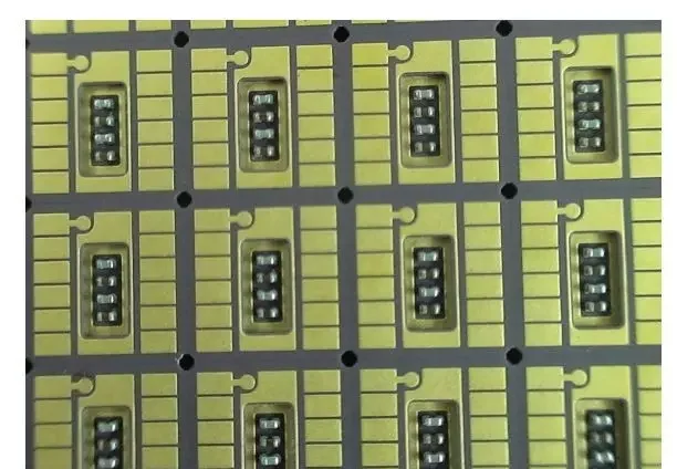
A Cavity PCB, short for Cavity Printed Circuit Board, is a specialized type of PCB that features one or more cavities or recesses within the board itself. These cavities are created by removing specific sections of the PCB substrate material, which can be made of materials like FR – 4, Rogers, or other substrates
Types of Cavity PCBs
- Blind Cavity PCBs: These have cavities that do not penetrate through the entire PCB. They are ideal for applications where components need to be partially embedded while maintaining a flat surface on the opposite side of the board. For example, in mobile devices, various components like the camera module or sensors can be partially recessed into the PCB to achieve a sleek, flat design.
- 2.Buried Cavity PCBs: The cavities in these PCBs are entirely enclosed within the board and do not extend to the outer layers. This design is often used to reduce the overall thickness of the PCB and protect sensitive components. In high – density electronics such as high – performance laptops or medical devices, designers use buried cavity PCBs to create a thinner profile without compromising the integrity of the components.
- 3.Through Cavity PCBs: Their cavities extend from one side of the board to the other, providing easy access for component placement and removal. They are commonly used in applications where components need to be mounted on both sides of the PCB, like in telecommunications equipment where space is limited
Advantages of Cavity PCBs
Reduced Profile: By embedding components within the PCB, cavity PCBs can reduce the overall height of a device. This is particularly useful in applications with strict space constraints, such as in the automotive industry for sleek, low – profile infotainment systems.
Enhanced Thermal Management: They can help in dissipating heat generated by embedded components more effectively, as the PCB itself can act as a heat sink
How are cavity PCBs manufactured compared to traditional PCBs?
Cavity PCBs are manufactured differently from traditional PCBs in several key aspects:
Design and Pattern Creation
- Cavity PCBs:
- Cavity Formation: The design process for cavity PCBs involves creating cavities or recesses in the PCB substrate. This is typically done by removing specific sections of the substrate material. For example, in the manufacturing of a cavity PCB, after the initial design, specific areas of the substrate are etched away to form the cavities. The pattern of these cavities is precisely controlled to house electronic components. The process may use techniques like photolithography, where a photoresist is applied, exposed to UV light through a photomask with the cavity pattern, and then developed to create the desired pattern on the substrate.
- Design Considerations: Designers need to carefully consider the size, shape, and location of the cavities to ensure proper component placement and functionality. They also need to take into account the electrical performance and thermal management requirements. For instance, in a high – density electronic device, the cavities may be designed to optimize the placement of high – power components to improve heat dissipation.
- Traditional PCBs: In contrast, traditional PCBs usually have a flat surface without such recesses. The design mainly focuses on the layout of components and the routing of electrical connections on a single – layer or multi – layer non – conductive substrate. The design process is more about optimizing the two – dimensional space for component placement and ensuring the electrical connections are correct.
Substrate Preparation
- Cavity PCBs: The substrate material for cavity PCBs needs to be carefully selected not only for its electrical properties but also for its machinability. Materials like FR – 4, Rogers, or other substrates are commonly used. After selecting the material, it is cut and cleaned to ensure a smooth and clean surface for further processing. The substrate must be able to withstand the etching process used to create the cavities without excessive damage or deformation.
- Traditional PCBs: Traditional PCBs also start with a non – conductive substrate, but the substrate selection is more focused on general electrical insulation and mechanical support. The substrate is typically made of materials such as fiberglass or epoxy resin. The preparation process mainly involves cutting the substrate to the required size and ensuring its surface is clean and free of impurities.
Component Placement and Assembly
- Cavity PCBs:
- Component Embedding: One of the significant differences is the ability to embed components within the cavities. This requires specialized equipment and techniques for precise placement. For example, in the case of blind cavity PCBs, components can be partially embedded while maintaining a flat surface on the opposite side. In the manufacturing process, after the cavities are created, components are placed into the cavities using pick – and – place machines. The placement accuracy is crucial to ensure the proper functioning of the circuit.
- Encapsulation: Once the components are placed in the cavities, they are often encapsulated to protect them from external factors such as moisture, dust, and mechanical stress. This encapsulation process can be done using various materials such as epoxy resins.
- Traditional PCBs: In traditional PCBs, components are typically placed on the surface of the board. The placement is done using pick – and – place machines, but there is no need for the additional step of embedding components into cavities. The focus is on ensuring that the components are correctly positioned on the surface of the board according to the design layout.
Manufacturing Challenges and Considerations
- Cavity PCBs:
- Etching Accuracy: The etching process for creating cavities needs to be highly accurate to achieve the desired cavity dimensions. Any deviation in the etching process can lead to cavities that are too large or too small, which can affect the component placement and the overall performance of the PCB.
- Thermal Management: While cavity PCBs offer better heat dissipation potential, the manufacturing process must also ensure that the heat generated by the embedded components can be effectively dissipated. This may require additional design considerations such as the use of heat – conducting materials or the optimization of the cavity structure.
- Traditional PCBs: Traditional PCBs face challenges such as ensuring the uniformity of the copper layer thickness and the accuracy of the hole drilling. The manufacturing process needs to ensure that the electrical conductivity of the copper traces is consistent and that the holes are drilled accurately to accommodate the component leads and vias.
Testing and Inspection
- Cavity PCBs: Due to the presence of cavities and embedded components, the testing and inspection process for cavity PCBs is more complex. Specialized testing equipment and techniques are required to ensure that the components are correctly placed and functioning within the cavities. For example, X – ray inspection may be used to check the integrity of the solder joints inside the cavities.
- Traditional PCBs: Traditional PCBs are also subject to testing and inspection, but the focus is mainly on checking the electrical connectivity, solder quality, and the absence of defects on the surface of the board. The testing methods are relatively more straightforward compared to cavity PCBs.