Understanding Cold Solder Joints in PCB Assembly
Table of Contents
Understanding Cold Solder, False Solder, Insufficient Solder, and Open Solder in SMT
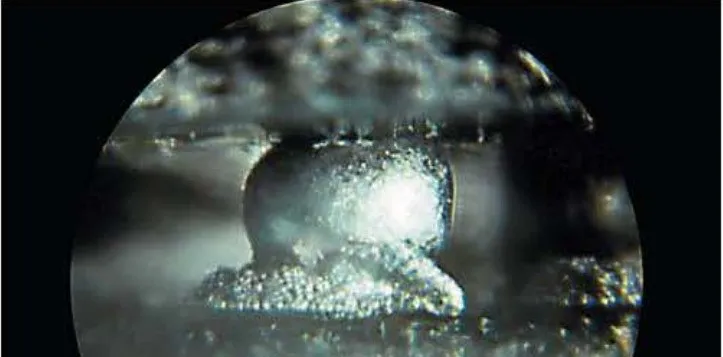
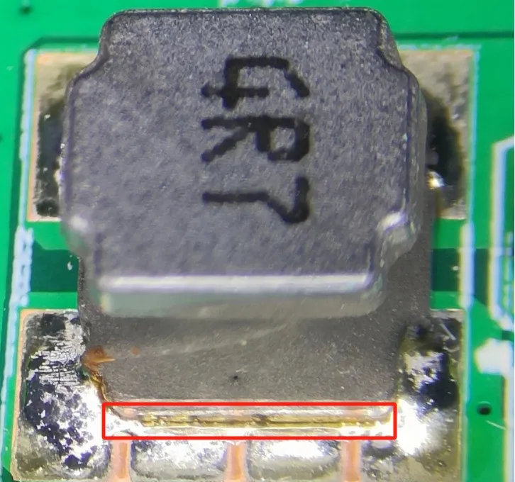
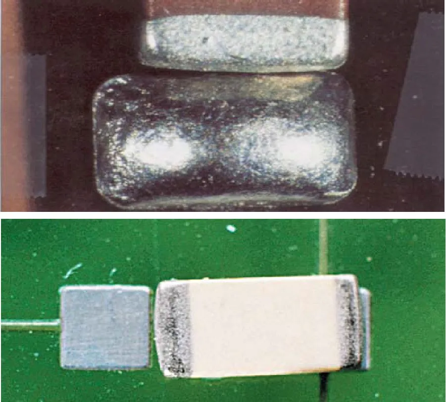
Cold soldering occurs when the solder joint between the component lead and the pad does not form a proper metallurgical bond. Visually, the surface appears rough, dull, and grainy — resembling unmelted solder powder. This is commonly referred to as “raw solder” or “semi-molten solder.”
Typical Causes:
Insufficient heat during the reflow process.
Excessive preheat duration.
Inadequate peak reflow temperature or insufficient time above liquidus.
Poor solderability of components or pads.
Surface contamination or oxidation.
Low-activity flux or degraded solder paste.
Improper PCB pad design.
Reflow Process Parameters:
For Sn63/Pb37 (Eutectic Solder):
Recommended peak temperature: ~215°C.
Time above 183°C (liquidus): 30–90 seconds.
For Lead-Free SAC305 Solder:
Recommended peak temperature: 235–242°C.
Time above 217°C (liquidus): 40–100 seconds.
Cold Solder Improvement Measures:
Optimize Reflow Profile:
Ensure sufficient heating in the soak and peak zones.
Monitor actual component and pad temperatures using thermocouples.
Improve Solder Paste Quality:
Avoid solder pastes with excessive oxide content or degraded activity.
Use fresh, well-stored solder paste with appropriate metal-to-flux ratio.
Ensure Clean Surfaces:
Clean any plating residues or oxidation from pads and component leads.
Strengthen post-electroplating cleaning procedures.
Improve Pad Design:
For NSMD (Non-Solder Mask Defined) pads, reduce thermal dissipation by minimizing pad connections to large copper areas such as GND.
Consider using thermal relief structures.
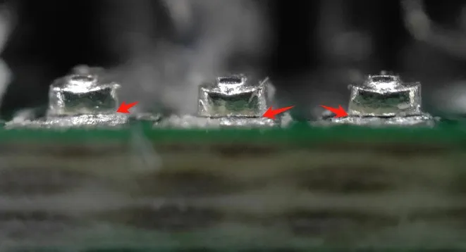
Grapeballing Effect (A Type of Cold Solder)
Grapeballing refers to the formation of isolated solder balls that do not coalesce into the main solder joint, commonly classified under cold solder defects.
Root Causes of Grapeballing:
Excessively long preheat zone in the reflow profile, leading to premature flux exhaustion.
Oxide layers on solder powder preventing proper melting and bonding.
Poor solder paste activity.
Inappropriate environmental temperature and humidity (MSD/MSL sensitivity).
PCB surface contamination.
Poor pad design (SMD vs NSMD, copper area).
Improper stencil design (violating IPC-7525 guidelines).
Fine-pitch components (01005/0201) with reduced solder volume and faster flux burnout.
Poor solder paste storage or selection (halogenated vs halogen-free).
Inadequate thermal transfer or inconsistent heating due to poor oven setup or card jamming.
False Solder (False Joint)
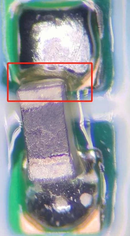
False solder joints appear to be properly soldered on the surface but lack any true metallurgical bonding. The joint can easily be pulled apart, indicating no actual solder fusion occurred between the pin and pad.
Causes:
Inadequate cleaning of the pad or component surfaces.
Use of insufficient or low-activity flux.
Solder paste dried out before reflow.
Contamination or oxidation on the lead or pad surfaces.
Identification Tip:
A false solder joint might appear visually acceptable but will fail mechanical stress or continuity tests. IPC-A-610 visual inspection standards may not catch these unless cross-sectional analysis or pull testing is conducted.
Insufficient Solder (Weak Joint)
Occurs when too little solder is present at the joint, resulting in unreliable electrical connectivity. The solder may not adequately bridge the component lead and pad, leading to intermittent open circuits during testing.
Causes:
Inadequate solder paste volume printed.
Low solderability of the component or pad.
Component shifting or tombstoning.
Flux burnout or oxidation during preheat.
Symptoms:
Joint appears minimal or poorly wetted.
Open or intermittent signals in electrical tests.
High failure rate during in-circuit or functional tests.
Open Solder Joint (No Solder Joint)
An open solder joint refers to a pad where soldering should have occurred but is completely missing. This results in a clear electrical discontinuity and can be visually confirmed during optical inspection.
Causes:
Insufficient solder paste printing or stencil blockage.
Component misplacement.
Extended delay between paste printing and component placement.
PCB or component defects.
Design Recommendations and Process Optimization
PCB Layout:
Optimize pad size and shape based on IPC-7351 and IPC-7525.
Use NSMD pads for better solderability unless thermal control is a priority.
Use thermal reliefs for pads connected to large copper areas.
Stencil Design:
Follow recommended area and aspect ratios.
Match stencil aperture design to component footprint.
Ensure proper alignment and cleaning to avoid blockage.
Reflow Oven Settings:
Use appropriate reflow profiles tailored to the solder paste and component density.
Choose the correct atmosphere: air, nitrogen, or vacuum.
Monitor conveyor speed, zone temperatures, and board dwell time.
Reference Standards
IPC-A-610: Acceptability of Electronic Assemblies.
IPC-7525: Guidelines for stencil design.
IPC-7351: SMD land pattern design standards.

Barry Ding
SEO
Email
WhatsApp
LinkedIn
Facebook
Contact me
About us
We are Yongchangtai Electronics — your trusted partner in high-quality PCB & PCBA manufacturing, backed by 15+ years of expertise and industry-leading capabilities.
Contact us
to Begin your Bessiness