PCBA Inspection and Acceptance
Table of Contents
Facebook
LinkedIn
Reddit
X
PCBA Inspection and Acceptance Criteria: A Comprehensive Guide
Why PCBA Inspection Matters
Modern PCBA inspection is more than a quality gate; it is the backbone of product reliability, safety, and brand trust.
Reliability – Detects early faults so assemblies survive the full service life—even in harsh automotive or industrial controls.
Safety – Prevents latent defects that could endanger patients, drivers, or flight crews.
Compliance – Confirms boards meet IPC-A-610 and customer-specific PCBA acceptance criteria, avoiding legal or market barriers.
Cost control – Fixing issues during PCB assembly inspection is far cheaper than field recalls.
Brand reputation – Consistent quality turns first-time buyers into long-term partners.
Core PCBA Inspection & Test Methods
| Method | Key Focus | Typical Long-Tail Keyword |
|---|---|---|
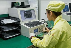
| Manual / Visual Inspection | Cracks, scratches, solder bridges, polarity errors | visual PCBA inspection checklist |
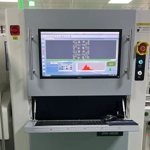
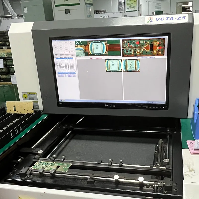
| AOI Inspection PCB | High-speed cameras flag missing parts, tombstones, insufficient solder | automated optical inspection PCBA |
| Solder Paste Inspection SPI | Measures paste height, volume, offset before placement | solder paste inspection SPI guidelines |
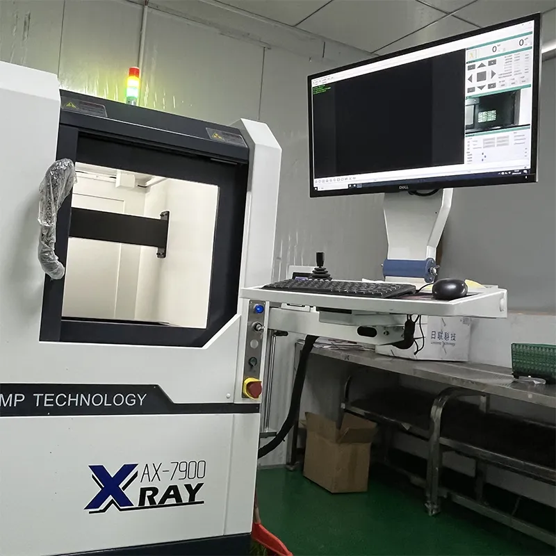
| X-ray BGA Inspection | Finds hidden voids, open joints, inner-layer shorts | X-ray BGA inspection standards |
| ICT (In-Circuit Test) | Nets continuity, resistance, short-open faults | in-circuit test PCBA |
| Functional Test PCBA | Powers board under simulated load to verify firmware, I/O, comms | PCBA functional test procedure |
| Environmental Reliability Testing | Thermal cycling, vibration, high-humidity aging | environmental reliability testing PCBA |
IPC-A-610 Classes & Acceptance Thresholds
| Class | Typical Application | Quality Expectation |
|---|---|---|
| 1 | Toys, low-cost consumer gadgets | Function over appearance |
| 2 | Computers, industrial controllers | Continuous performance, moderate lifetime |
| 3 | Medical, aerospace, automotive safety | Zero-defect mindset, critical reliability |
Appearance & Cleanliness
No surface scratches, warpage or oxidation.
Flux, dust, and fingerprints removed; legend printing legible.
Solder-Joint Quality
Fillets full, shiny, well-wetted.
No voids, cracks, cold joints, or bridges.
Solder volume meets pad-size guidelines.
Component Placement
- Position and polarity correct; no tombstones, lifted leads, or misalignment.
Board Dimensions & Integrity
- Outline, holes, and cut-outs within tolerance; bow/ twist ≤ 1.5 % of length.
Electrical & Functional Performance
- Pass continuity, insulation-resistance, impedance tests; firmware boots; interfaces respond.
Environmental Reliability
- Boards withstand thermal shock, humidity, vibration with no function loss.
Defect Categories & AQL Electronics Levels
| Defect Level | Description | Typical AQL |
|---|---|---|
| Critical (CR) | Safety-related, may cause injury or catastrophic failure | 0 % |
| Major (MA) | Affects function or life | 0.4 % |
| Minor (MI) | Cosmetic only | 0.65 % |
Critical defects are never accepted; major ones trigger rework; minor issues have limited tolerance in Class 1.
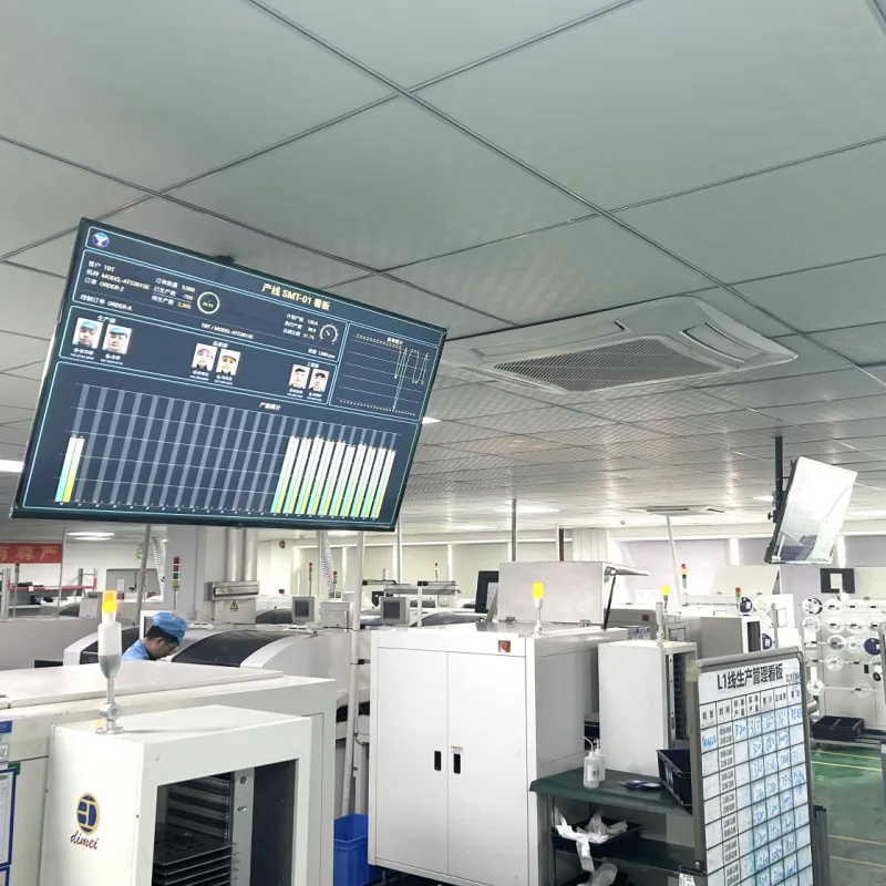
Typical End-to-End PCBA Inspection Flow
Incoming Material Check – Bare PCB and component validation.
Solder Paste Inspection SPI – Early control of volume/ alignment.
Pre-reflow AOI Inspection PCB – Confirms part presence & orientation.
Reflow – Controlled thermal profile.
Post-reflow AOI – Flags bridges, cold joints, solder voids.
Manual Sampling – Human eyes cover AOI blind spots.
X-ray BGA Inspection – Deep look at hidden solder balls.
ICT – Electrical shorts/opens, component values.
Functional Test PCBA – Real-world simulation.
Final Visual Audit – Silkscreen, labeling, packaging.
Environmental Reliability Testing – High-stress proof if required.
Common PCBA Defects & Root Causes
Soldering Defects
Cold joint – Dull, grainy surface from inadequate heat or oxidised pads.
Solder bridge – Excess paste or tight pitch.
Insufficient solder – Under-printed paste or poor plating.
Voids – Moist laminate, volatile solvents, wrong reflow profile.
Tombstone – Uneven heating or asymmetrical pad design.
Component Issues
Misplacement, polarity reversal, missing parts, lifted leads—often due to pick-and-place program errors or vibration.
Board-Level Problems
Delamination – Moisture or over-curing.
Warping – Uneven copper, stacking stress, improper storage.
Contamination – Flux residues attract moisture leakage.
Best Practices for High-Yield PCBA Inspection
| Pillar | Actions & Embedded Long-Tail Keywords |
|---|---|
| Design for Manufacturability (DFM for PCB assembly) | Size pads per IPC-7351, leave ICT pads, avoid tall part shadows. |
| Process Control & SPC | Monitor paste height in real time; track PPM trends to spot drifts. |
| Equipment Calibration | Schedule AOI, SPI, X-ray accuracy checks every quarter. |
| Training to IPC-A-610 | Certify operators; refresh when standards update. |
| Traceability | Barcode or RFID every board; log defects and rework to aid continuous improvement. |
PCBA Inspection Quick-Reference Checklist


| Item | Pass Criteria |
|---|---|
| Appearance | No scratches, warps, discoloration, foreign matter. |
| Solder Joints | Smooth, convex, fully wet, no voids or cracks. |
| Components | Correct value, orientation, spacing; no tombstones or missing parts. |
| Dimensions | PCB size within ±0.13 mm; bow/twist ≤ 1.5 %. |
| Electrical Tests | Continuity, insulation-resistance, impedance OK. |
| Functional Tests | All I/O respond; firmware loads; interfaces stable. |
| Environmental Tests | Survive specified temperature, humidity, vibration without degradation. |
Conclusion
Robust PCBA testing—combining SPI, AOI, X-ray, ICT, functional and environmental checks—ensures every assembly meets strict PCBA acceptance criteria. By aligning with IPC-A-610 Class requirements, leveraging AQL electronics guidelines, and enforcing traceable process control, manufacturers slash defect rates and secure long-term customer trust.
PCBAYCT integrates inspection into every design-for-manufacture stage, employs real-time data analytics, and offers full traceability to guarantee Class 3-level reliability.
Ready to elevate your board quality? Contact PCBAYCT for a free DFM review and see how our end-to-end PCBA inspection program can safeguard your next project.

Barry Ding
CEO
Email
WhatsApp
Facebook
Phone
Contact me
About us
We are PCBAYCT Electronics — your trusted partner in high-quality PCB & PCBA manufacturing, backed by 15+ years of expertise and industry-leading capabilities.
Contact Us
to Begin Your Bessiness