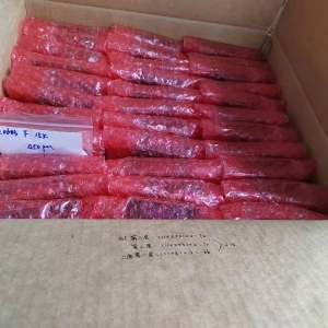
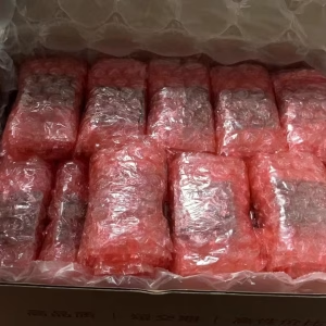
PCB Assemble Process
Surface Mount Assembly Process
Historically, all printed circuit boards (PCBs) were assembled manually using only a soldering iron. However, with advancements in technology, components have become smaller and more complex, making hand assembly increasingly challenging. Additionally, the number of components that can fit on a single board has grown significantly. As a result, the development of automated assembly processes became essential to meet the demands of modern electronics manufacturing.
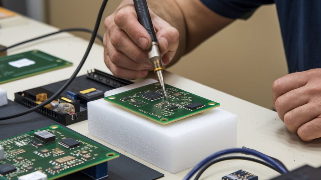
Required Elements
To facilitate automated assembly, the following components are required:
Gerber Files: Provided in 274-X format (with embedded apertures), including the fabrication drawing. These files define pad locations, help the assembly house identify the location of pin 1, and provide a visual representation of the board layout.
Part Centroid Text File: This should include reference designators, an external placement layer, and the X & Y coordinates along with rotation in ASCII format. This file is essential for determining where each component will be placed on the PCB.
Numerical Control (NC) Drill Files: Used to locate mounting holes and specify sizes for through-hole components, ensuring the assembly house maintains adequate clearance for component leads.
Solder Paste File: This is one of the Gerber files required for all sides mounted. It masks the entire board except for the areas needing solder. The solder paste is applied to exposed pads, and the stencil is removed, allowing components to be held in place by the paste and glue dots during soldering.
Glue Dot File: This file specifies where glue dots will be applied to secure components during assembly.
Design Database: If available, provide the design database along with its format and program name. This database helps in determining the location of pin 1 and serves as a reference for the assembly process.
Parts List or Bill of Materials (BOM) : This list should detail the components to be mounted, including their designators in reference to the centroid file, and specify whether they are surface mount (SMT) or through-hole components.
For optimal results, consistency in the rotation of original components is crucial. Unless the designer’s software can manage variations, all components should be oriented similarly.
Providing these essential elements ensures a smooth and efficient automated assembly process, helping achieve high-quality results with each PCB developed.
Other Considerations
When it comes to automated PCB assembly, several critical factors play a significant role in ensuring efficiency, quality, and effectiveness. Among these, board size, panel size, and breakaway connections are paramount:
Board Size:
- Standardization: The dimensions of the PCB are crucial, as they must conform to industry standards or specific project requirements. Common sizes can vary based on applications, from small modules used in mobile devices to larger boards used in industrial machinery.
- Component Layout: The board size directly impacts the layout of components. Designers must consider the arrangement of components to optimize space while ensuring accessibility for soldering and testing.
- Heat Management: Smaller boards may face challenges regarding heat dissipation, while larger boards may require careful considerations to ensure uniform thermal management across components.
Panel Size:
- Efficiency in Production: PCBs are typically assembled in panels that contain multiple boards, which allows for batch processing. This setup maximizes the use of space during manufacturing and minimizes costs by reducing handling time and equipment setup.
- Optimized Panel Design: The panel’s design often reflects the etching and routing strategy utilized prior to assembly. Panelization must balance between maximizing the number of boards per panel and ensuring ease of separation after assembly.
- Transport and Handling: Larger panels can be cumbersome to handle, transport, and store, potentially leading to damage. Thus, the choice of panel size should take into account logistics and operational capabilities.
Breakaways:
- Definition and Purpose: Breakaways are strategically placed connections around each board within a panel that holds the boards securely during assembly. These connections are designed to maintain structural integrity while facilitating the assembly process.
- Ease of Separation: The unique design of breakaways allows for easy detachment of individual boards from the panel once assembly is complete. This is critical in ensuring that the boards can be removed without causing damage to the solder joints or the board itself.
- Quality Assurance: Properly designed breakaways can also contribute to quality assurance during assembly. They provide stability to the boards as they undergo various processes such as solder paste printing, reflow soldering, and inspection.
By considering the board size, panel size, and breakaway design, PCB designers and manufacturers can optimize the automated assembly process to produce high-quality, reliable products efficiently.
1.Ordering a Board
PCBATop One-Stop Solution for PCB & Prototype Assembly
2.DFM Check
Identification of Design Flaws:
- The DFM check meticulously examines the PCB design for any missing, redundant, or potentially problematic features. It scrutinizes various aspects of the design including component placement, trace width, hole sizes, and layer stack-up.
- Example issues may include:
- Insufficient Spacing: Inadequate spacing between components can lead to electrical shorts, signal interference, or physical obstructions during assembly. Narrow gaps may prevent proper soldering, resulting in poor electrical connections.
- Inappropriate Component Selection: Using components that do not fit within the design constraints or are difficult to source can lead to delays during production.
- Complexity: Overly complex designs can increase manufacturing time and cost, as well as heightening the risk of errors.
Enhancing Functionality:
- By addressing design flaws during the DFM check, manufacturers can improve the overall functionality of the final product. This proactive approach helps prevent issues that may arise after production, such as overheating, unintentional grounding, or device malfunctions.
Cost Reduction:
- A thorough DFM check significantly cuts manufacturing costs by minimizing the likelihood of scrapping boards due to design-related failures. Unforeseen expenses arising from rework, repairs, or redesign are substantially reduced.
- By optimizing the design for manufacturability, companies can streamline production processes, making them faster and more efficient. This, in turn, leads to lower labor costs and reduced material waste.
Quality Assurance Commitment:
- The DFM process is integral to our commitment to providing high-quality PCBs at competitive prices. It reflects our dedication to excellence by ensuring that every design adheres to the best manufacturing practices.
- Ensuring that designs are DFM-compliant not only enhances the reliability of the final product but also fosters confidence among clients, reinforcing their trust in our capabilities.
3.Incoming Quality Control(IQC)
At PCBATop, our commitment to quality begins well before the assembly process. The Incoming Quality Control (IQC) phase is critical, as it ensures that all materials received meet our stringent standards before we proceed with Surface Mount Technology (SMT) assembly. This proactive approach helps us mitigate potential issues and maintain the integrity of the final product.
- Verification of Model Numbers and Quantities:
- Each shipment undergoes a meticulous verification process to ensure that the model numbers and quantities match the specifications outlined in the Bill of Materials (BOM) . This is crucial not only for maintaining inventory accuracy but also for ensuring that all necessary components are available for the production run.
- Discrepancies in model numbers or quantities are flagged for immediate resolution, ensuring that we only work with correct and complete materials.
- Physical Condition Inspection:
- We conduct thorough inspections of incoming materials to check for any signs of damage or defects. This includes assessing the shape and condition of components, particularly focusing on:
- Deformation: Components that do not maintain their intended shape may lead to assembly errors or functionality issues.
- Broken Pins: Damaged pins on Integrated Circuits (ICs) and other components can hinder connectivity and lead to product failures.
- Oxidation: Oxidized surfaces can create poor connections and degrade performance, making it essential for components to be visually and physically free from such issues.
- We conduct thorough inspections of incoming materials to check for any signs of damage or defects. This includes assessing the shape and condition of components, particularly focusing on:
- Sample Testing:
- To further ensure quality, we perform sample testing of incoming materials using specialized tools, such as:
- Test Frames: These tools help verify the electrical performance of components, ensuring they meet specifications.
- Multimeters: Used for measuring electrical properties, multimeters assist in confirming the functionality of critical components before they enter the assembly line.
- This testing phase helps identify any latent defects that might not be visible during initial inspections, thus enhancing our overall quality assurance efforts.
- To further ensure quality, we perform sample testing of incoming materials using specialized tools, such as:
- Handling Defective Materials:
- In the event that defects or discrepancies are discovered during the IQC process, we take immediate action. Our policy is to return defective materials to the supplier or customer in accordance with our quality management procedures. This not only protects the integrity of our manufacturing process but also fosters accountability and transparency in our supply chain.
4.Machine programming – Gerber / CAD to Centroid / Placement / XY file
After receiving the PCB panels and components, the subsequent step in the automated assembly process is to set up the various machines that will facilitate manufacturing. This step is crucial for ensuring that the assembly process operates smoothly and efficiently, ultimately contributing to high-quality production outcomes.
Placement Machine:
- Role in Assembly: The placement machine is responsible for accurately positioning and affixing surface mount components onto the solder-pasted pads of the PCB. Precision in this step is vital, as the performance and reliability of the final product depend heavily on proper component placement.
- Programming Requirements: To function effectively, each placement machine requires specific programming that dictates the coordinates and orientation for each component. Typically, this data is derived from CAD drawings, which provide detailed information about the layout and specifications of the PCB.
- Challenges with Data Availability: Unfortunately, CAD data is not always readily available from clients or design teams. When it is missing, alternative data sources must be utilized.
Automated Optical Inspection (AOI) Machine:
- Purpose in the Process: AOI machines are utilized at various stages throughout the assembly process to ensure the quality of the components placed on the PCB. They check for correct placement, orientation, and any potential defects that could arise.
- Programming and Data Utilization: Like placement machines, AOI systems also require precise programming. This programming is generally best generated from CAD data, as it allows for an exact match between the design specifications and the placement verification.
Utilizing Gerber Data:
- Availability of Gerber Files: In the absence of CAD data, Gerber files—commonly available following PCB fabrication—serve as a critical alternative resource. Gerber files contain extensive information about the PCB layout, including pad locations, traces, and routing, making them instrumental in both the manufacturing and inspection phases.
- Adapting Gerber Data for Machine Programming: While Gerber files do not directly indicate component placements, they provide essential information about the PCB’s physical characteristics. Manufacturers can use Gerber data along with additional component placement data (such as centroid files) to create the necessary machine programs for both placement and inspection.
Integration into Workflow:
- Streamlined Approach: By integrating machine setup processes effectively, we can minimize downtime and ensure that assembly lines operate at optimal efficiency. A systematic approach to programming and setting up each machine contributes to smoother transitions through different stages of assembly.
- Continuous Improvement: Constant evaluation and adjustment of the machine setups will lead to enhanced precision and speed in the production process. Regular updates to programming based on feedback and inspection results will help sustain high standards of quality.
5.Solder Paste Printing
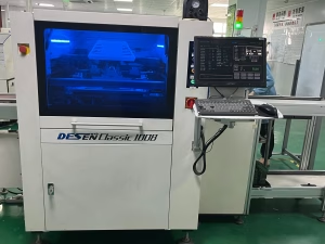
The first machine to setup in the manufacturing process is the solder paste printer which is designed to apply solder paste using a stencil and squeegees to the appropriate pads on the PCB.
6.Component Placement
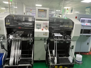
After verifying that the printed PCB has the correct amount of solder paste applied, the assembly process moves into the crucial phase of component placement. This step involves the precise positioning of electronic components onto the solder-pasted pads of the PCB, ensuring they are ready for soldering.
7.Pre-Reflow Automated Optical Inspection (AOI)
Once the component placement process is complete, it is essential to verify that all components have been accurately positioned on the PCB prior to reflow soldering. This verification step is crucial for ensuring the integrity of the assembly and preventing issues that could lead to product failure. The most effective method for conducting this verification is through Automated Optical Inspection (AOI) .
Component Presence Check:
- The AOI machine performs an initial check to confirm that all components are present on the PCB. This helps identify any missing components that could impact functionality.
- By comparing the actual placements to the programmed data, the AOI can quickly detect discrepancies.
Type and Value Verification:
- The AOI system is capable of recognizing different component types and values (e.g., resistors, capacitors, ICs) through visual inspection. It uses advanced image recognition algorithms to ensure that the correct parts are placed in their designated positions.
- This step mitigates the risk of cross-references leading to the wrong components being mounted, which could adversely affect circuit performance.
Polarity Checks:
- Certain components, such as diodes and electrolytic capacitors, have polarity that must be observed for correct operation. The AOI machine can verify that these components are oriented correctly before the reflow process begins.
- Ensuring that polarized components are placed accurately is critical to avoiding potential failures in the circuit.
Quality Assurance:
- Along with confirming component presence, type, and orientation, the AOI can also inspect for physical defects such as:
- Misalignment of components
- Incorrect solder paste application (e.g., excessive spillage)
- Component damage during the placement process
- By identifying these issues early, manufacturers can address them before proceeding to the costly reflow soldering stage.
- Along with confirming component presence, type, and orientation, the AOI can also inspect for physical defects such as:
8.Reflow Soldering
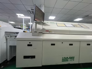
After components have been accurately placed on the PCBs, they are sent through reflow machines to solidify the solder paste and permanently attach the components to the board. This process is known as reflow soldering, and while it may seem straightforward, it involves critical considerations to ensure effective and reliable solder joints.
Purpose of Reflow Soldering:
- Reflow soldering serves to melt the solder paste, allowing it to flow and bond the surface mount components to the PCB pads. Once cooled, the solder solidifies, creating strong mechanical and electrical connections.
- This method is widely preferred for its ability to efficiently solder numerous components in a single pass while ensuring uniform processing across the board.
Importance of the Reflow Profile:
- The reflow profile refers to the specific temperature and timing settings used during the reflow cycle. Achieving the correct profile is crucial for optimal solder joint quality and preventing damage to components.
- Proper profile design includes several temperature stages:
- Preheat Stage: Gradually raises the temperature to avoid thermal shock to the components, allowing the solder paste to activate and begin to flow.
- Reflow Stage: Reaches the peak temperature where solder melts and forms the joints; this temperature needs to be carefully controlled.
- Cooling Stage: Rapidly cools down to solidify the solder, ensuring that the joint maintains integrity.
Challenges with Lead-Free Solder:
- With the transition to lead-free solder, the importance of precise reflow profiles becomes even more pronounced. Lead-free solders typically have higher melting points, which means that the reflow temperature must be managed closely to avoid exceeding the maximum rated temperatures of components.
- Components may have different maximum temperature ratings. Therefore, the reflow profile must ensure that:
- All components are subjected to enough heat to properly solder while avoiding excessive heat that could lead to damage, delamination, or other failures.
- The thermal mass of the PCB and the components must be considered, as varying sizes and materials can affect the heating and cooling patterns.
Process Monitoring and Adjustments:
- Continuous monitoring of the reflow process is crucial. Many modern reflow ovens are equipped with profiling tools that allow operators to measure and record temperature distributions during every cycle.
- Adjustments may need to be made based on real-time feedback to meet desired profile criteria, ensuring that every board is processed within acceptable parameters.
Final Inspection and Testing:
- After reflow soldering, it’s essential to inspect the solder joints for quality. Typical checks include verifying joint appearances, using techniques like X-ray inspection or cross-sectional analysis to examine internal structures.
- Quality assurance tests can include functional testing to ensure that the electrical connections are sound and the assembly operates as intended.
9.Post-Reflow Automated Optical Inspection (AOI)
Once the reflow soldering process is completed, it is essential to perform a thorough inspection to verify that no mistakes were made during assembly. This last step is critical to ensuring the reliability and functionality of the PCB. The inspection may reveal issues such as poor solder joint quality, misalignment due to movement during reflow, or unintended electrical shorts caused by misplaced components.
Manual Checks:
- Manual inspection involves operators visually examining the solder joints and component placements on the PCB.
- Although this method can be effective for detecting obvious defects, it is labor-intensive and susceptible to human error, especially in high-volume production environments.
- Manual checks can be complemented with tools like magnifying glasses or lighted inspection stations to enhance visibility.
Automated Optical Inspection (AOI) :
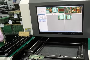
- AOI is a widely adopted inspection method that employs high-resolution cameras and advanced image processing algorithms to analyze the PCBs for defects.
- Key Functions of AOI:
- Solder Joint Quality: AOI can assess the integrity of solder joints, detecting defects such as insufficient solder, solder bridges, and cold solder joints.
- Component Placement: It checks for correct component placement, verifying that each component is in its specified location and properly oriented.
- Visual Defects: AOI can identify physical imperfections such as scratches on the PCB, incorrect component types, or any foreign materials on the board.
- The speed and accuracy of AOI make it an effective solution for high-volume production, providing immediate feedback for quick corrective actions.
Automated X-Ray Inspection (AXI) :
- AXI is used for inspecting areas that may be difficult to assess visually, particularly for components with hidden features, such as BGAs (Ball Grid Arrays).
- Capabilities of AXI:
- Internal Joint Integrity: AXI can detect issues beneath components, such as voids or insufficient connections that are not visible from the surface.
- Short Circuits: The technology can identify shorts caused by solder bridging or misaligned components that connect unintended pads.
- Registration Verification: Ensures that components are correctly aligned and affixed to the PCB.
- AXI provides a non-destructive method for inspection, making it valuable for complex assemblies where component integrity is paramount.
10.Conformal Coating
Some completed Printed Circuit Board Assemblies have a conformal coating. It’s usually depends on the customer’s product requirements.
11.Final Inspection and Functional Test
Functional Testing in PCB Assembly
After completing the soldering and conformal coating processes, the assembled PCB undergoes a crucial final inspection known as the functional test. This stage is vital for verifying that the assembled PCB meets design specifications and performs as intended under normal operating conditions.
The primary objective of functional testing is to ensure that the PCB operates correctly and reliably in its intended application. This involves assessing the electrical performance of the PCB and confirming that all components function as designed.
Test Preparation:
- Prior to testing, the Quality Assurance (QA) team prepares the necessary equipment and software, which may be supplied by the customer or developed specifically for the project.
- PCBATop can create custom test fixtures tailored to the unique requirements of each customer’s PCB design. These fixtures facilitate the connection of the PCB to testing equipment and provide a stable environment during testing.
Testing Procedures:
- During the functional test, the PCB is subjected to a range of tests that simulate the normal operating conditions it will experience in its end use. These tests typically include:
- Power Tests: The PCB is powered on to check for correct voltage levels and current draws, ensuring that the power supply and regulation circuits are functioning properly.
- Signal Simulation: Testers inject simulated signals into the PCB to evaluate its response—this can involve digital inputs, analog signals, or communication protocols relevant to the application.
- Functional Checks: The test assesses the performance of specific components and circuits, verifying that sensors, actuators, and other functional elements operate correctly within their specified parameters.
- During the functional test, the PCB is subjected to a range of tests that simulate the normal operating conditions it will experience in its end use. These tests typically include:
Monitoring and Data Collection:
- During the testing phase, operators closely monitor the electrical characteristics of the PCB. They track key metrics such as:
- Voltage levels
- Signal integrity
- Timing characteristics
- Data logging tools are often used to record results for analysis, enabling troubleshooting and identification of any anomalies during testing.
- During the testing phase, operators closely monitor the electrical characteristics of the PCB. They track key metrics such as:
Error Detection and Troubleshooting:
- If the PCB fails any aspect of the functional test, the QA team investigates the cause of the failure. Potential issues may include:
- Solder joint defects
- Component malfunctions
- Design flaws
- Identifying and addressing these problems before final delivery ensures that customers receive high-quality, reliable products.
- If the PCB fails any aspect of the functional test, the QA team investigates the cause of the failure. Potential issues may include:
Passing Criteria:
- The criteria for passing the functional test are based on customer specifications and application requirements. A successful test indicates that the PCB meets the design’s electrical performance standards and is ready for deployment.
12.Washing and Drying
Cleanliness in PCB Manufacturing
The PCB manufacturing process is inherently prone to contamination, and maintaining cleanliness throughout the various stages is vital for ensuring high-quality assemblies. Contaminants from solder paste, human handling, and the environment can accumulate on the PCB surfaces, leading to both aesthetic concerns and practical issues that can impact the performance and reliability of the final product.
Sources of Contamination
Solder Paste Residue:
- Solder paste contains flux, which is essential for the soldering process as it helps to clean and facilitate good solder joints. However, leftover flux can create a sticky, greasy residue on the PCB after soldering.
- If not properly cleaned, flux residues can attract dust and dirt, leading to potential interference with board functionality.
Human Handling:
- Oils, dirt, and other contaminants from fingers and clothing can be transferred to the PCB surfaces during handling, particularly during assembly and inspection processes.
- These residues can lead to corrosion of metal surfaces and compromise electrical connections over time.
Environmental Factors:
- Particles from the ambient environment, such as dust and chemical residues, can settle on PCB surfaces during manufacturing, especially in less controlled environments.
Importance of Cleaning
Aesthetic Appeal:
- A clean PCB looks more professional and can enhance the perception of quality by customers. Visual imperfections may lead to a negative impression, even if the board functions correctly.
Functional Integrity:
- Contaminants can cause short circuits, increase resistance in electrical pathways, and hinder signal integrity by creating barriers to proper electrical contact.
- Cleaning ensures that all conductive and non-conductive surfaces are free from residues that could compromise performance.
Longevity and Reliability:
- Over time, contaminants can lead to corrosion and degradation of components, potentially resulting in failure during operation.
- Implementing effective cleaning processes enhances the integrity and longevity of the PCB, reducing the likelihood of field failures.
Cleaning Processes
To effectively remove contaminants, PCB manufacturers often implement the following cleaning processes:
Washing:
- PCBs may be washed using aqueous or solvent-based cleaning agents specifically designed to remove flux residues and other contaminants.
- Cleaning systems can include ultrasonic cleaning, immersion washing, or spray cleaning, depending on the level of contamination and manufacturer preferences.
Rinsing:
- After washing, thorough rinsing with deionized water or suitable solvents ensures the removal of cleaning agents, leaving the PCB surface clean and free of residue.
Drying:
- Proper drying methods, such as forced air or vacuum drying, are essential to remove any moisture and prevent the formation of water spots or residue.
Quality Control:
- Inspections are performed post-cleaning to ensure that the PCBs meet cleanliness standards. This may include visual inspection or testing for specific contaminants.
13.Packing and Shipping
