Features of Multi-layer PCB
Features of Multi-layer PCB
Multi-layer printed circuit boards (PCBs) have become the backbone of modern electronics, providing compact, reliable, and efficient solutions for complex electronic applications. This guide explores the key features of multi-layer PCBs and how they can benefit your projects and products.
What is a Multi-layer PCB?
A multi-layer PCB consists of more than two conductive layers (copper layers), separated by insulating layers (dielectric substrates). These layers are laminated together under high pressure and temperature, creating a robust and versatile circuit structure suitable for complex circuits and high-performance applications.

Key Features of Multi-layer PCBs
1. Increased Density and Compact Size
Multi-layer PCBs maximize space usage by allowing components to be mounted on both sides and enabling internal circuitry layers. This high-density design significantly reduces the overall PCB size without compromising performance.
2. Enhanced Electrical Performance
Multi-layer PCBs offer superior electrical performance due to shorter signal paths and reduced noise and interference. They are particularly beneficial for high-frequency circuits and advanced electronic devices.
3. Improved Signal Integrity
Internal ground and power layers within multi-layer PCBs help to minimize electromagnetic interference (EMI), thereby enhancing signal integrity and ensuring reliable performance in critical applications.
4. Greater Flexibility in Circuit Design
The multiple conductive layers provide designers with greater flexibility. Complex interconnections can be achieved without extensive wiring, simplifying the design process and facilitating advanced functionalities.
5. High Reliability and Durability
Due to their laminated structure, multi-layer PCBs exhibit excellent mechanical strength, thermal stability, and durability. These properties make them ideal for use in demanding environments and applications requiring high reliability.
6. Better Thermal Management
The additional layers help distribute heat evenly across the board, reducing hotspots and enhancing thermal performance. This feature is crucial for power-intensive applications.

7. Cost-Effective for Complex Circuits
Although multi-layer PCBs might have a higher initial cost, they are ultimately cost-effective for complex circuits by reducing assembly times, minimizing errors, and enhancing product reliability and longevity.
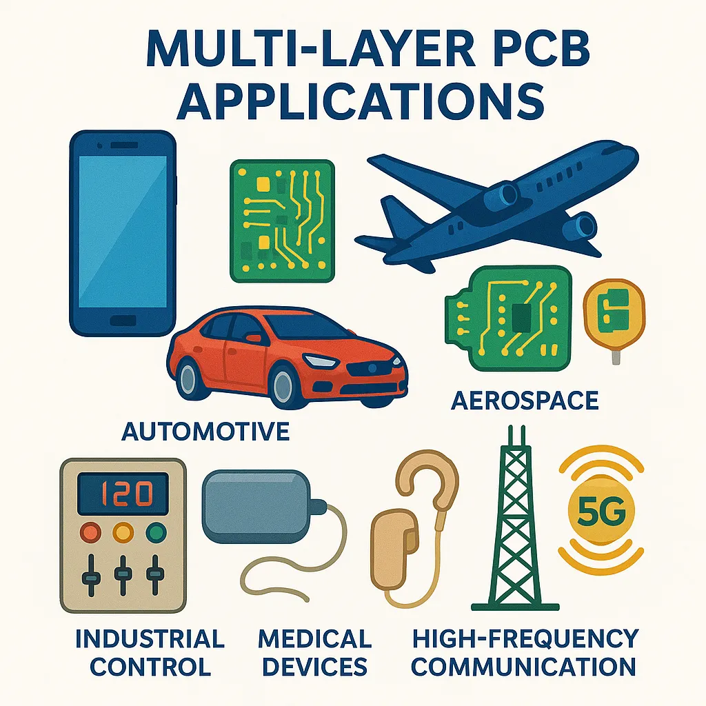
Typical Applications of Multi-layer PCBs
Multi-layer PCBs are widely used across numerous industries, including:
Consumer Electronics: Smartphones, tablets, and wearables.
Automotive: Advanced driver-assistance systems (ADAS), engine control units, and infotainment systems.
Medical Devices: Diagnostic equipment, imaging systems, and patient monitoring devices.
Aerospace and Defense: Communication systems, navigation equipment, and control systems.
Telecommunications: Network equipment, routers, and satellite communications.
Factors to Consider When Choosing Multi-layer PCBs
Number of Layers: Determined by the complexity and density of your circuitry.
Material Selection: Common materials include FR-4, polyimide, and high-frequency laminates.
Thickness and Layer Stack-up: Important for achieving desired electrical and thermal performance.
Manufacturing Capabilities: Ensure your PCB manufacturer has advanced facilities for high-quality, multi-layer production.
Conclusion
Multi-layer PCBs offer numerous benefits that make them indispensable for complex and high-performance electronic devices. By understanding these features and working with a capable PCB assembly partner, you can significantly enhance your product’s performance and reliability.
For expert multi-layer PCB assembly services, contact us today and elevate your electronics projects to the next level.