
Printed circuit board assembly (PCBA) is the process of soldering electronic components onto a bare PCB through Surface-Mount Technology (SMT) and Through-Hole Technology (THT) to create a fully functional electronic device. Often called “the heart” of modern electronics, a PCBA underpins everything from everyday consumer gadgets to aerospace and military systems.
PCB vs. PCBA
| Term | Definition |
|---|---|
| PCB (Printed Circuit Board) | A flat, non-conductive substrate etched with conductive copper traces. On its own, it has no functional capability. |
| PCBA (Printed Circuit Board Assembly) | A PCB that has completed component assembly and can perform a specific function. |
PCB Assembly Process
1. Design for Assembly (DFA) Review
Before production, engineers perform a DFA check to verify the Gerber files and bill of materials (BOM) for manufacturability. Key review points include:
- Component availability and correct specifications
- Package dimensions vs. actual parts
- Adequate spacing between components
- Accurate drill files and board outline
- Thermal-relief and other DFM/DFA guidelines
Early validation prevents costly errors and ensures a smooth build.
2. Solder-Paste Printing
A stainless-steel stencil and mechanical fixtures apply solder paste—a mixture of tiny solder spheres and flux—precisely onto each pad. The paste acts both as an adhesive and as the solder for later reflow.
3. Component Placement
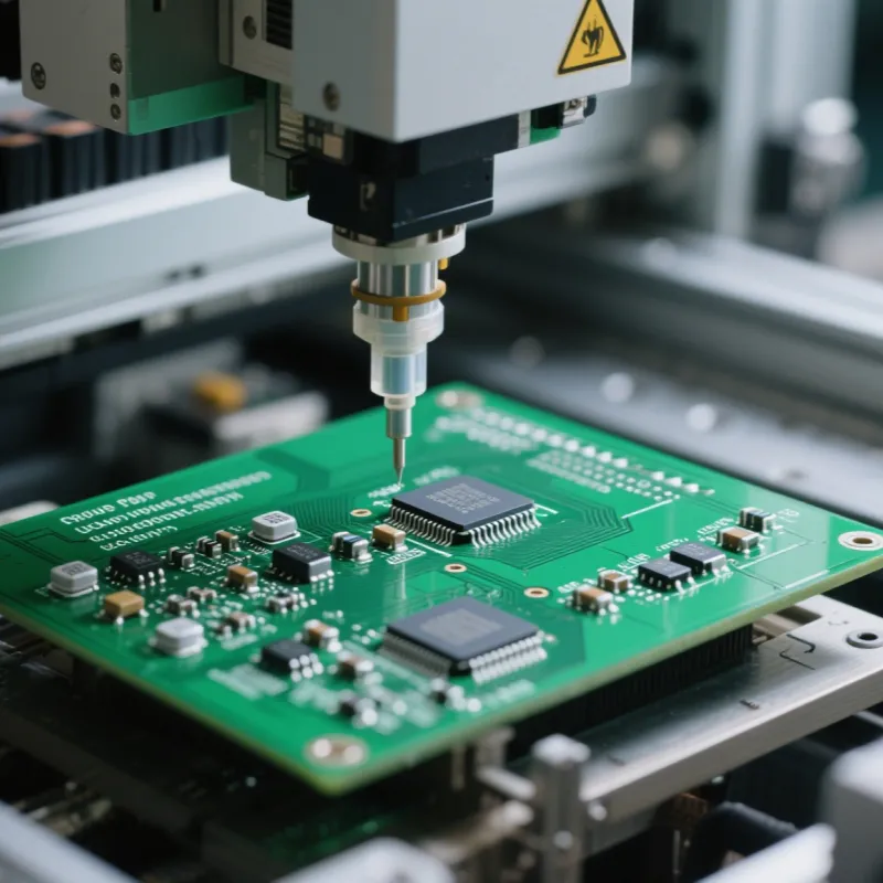
After paste deposition, Surface-Mount Devices (SMDs) are positioned by high-speed pick-and-place machines that use vision systems to achieve component-level accuracy—often tens of thousands of placements per hour.
THT parts that require leads inserted into plated through-holes are placed manually or by automated insertion systems when higher mechanical strength or specific packages demand it.
4. Soldering
Heating the solder paste forms permanent electrical and mechanical bonds:
- Reflow Soldering – The entire board passes through a reflow oven with a controlled thermal profile. Standard for SMT.
- Wave Soldering – The PCB rides over a wave of molten solder, ideal for high THT counts and some mixed-technology boards.
- Hand Soldering – Used for prototypes, small runs, or components unsuited to automated soldering.
5. Cleaning
Post-solder cleaning removes flux residues and contaminants that could affect reliability. Methods include aqueous wash, solvent cleaning, or a no-clean process chosen according to flux type and end-use.
6. Inspection & Quality Control
Robust QC ensures each board meets performance and reliability standards:
| Method | Purpose |
|---|---|
| Visual Inspection | Detects misalignment, missing parts, poor joints, or physical damage under magnification. |
| Automated Optical Inspection (AOI) | High-resolution cameras scan for placement errors, bridges, and insufficient solder. |
| X-Ray Inspection | Reveals hidden defects inside packages like BGAs and multilayer joints. |
| Functional Test | Powers the board and applies simulated signals to verify correct operation. |
7. THT Component Soldering
If THT parts are present, they are inserted and soldered—by hand for small volumes or via wave soldering for mass production.
8. Final Test & Shipment
A final round of inspection and functional testing catches any remaining defects. Passed boards are packaged for delivery; failed units are reworked or scrapped.
Assembly Techniques & Soldering Methods
- Reflow Soldering – Precise, reliable, SMT-centric.
- Wave Soldering – Efficient for THT and some SMT hybrids.
- Hand Soldering – Flexible for low volumes or special cases.
- Soft vs. Hard Soldering – Selected when exotic materials or higher joint strength is required.
Quality Control in PCBA
- Visual Inspection – Detects surface flaws and alignment issues.
- AOI & X-Ray – Identify hidden faults and verify placement accuracy.
- Functional Testing – Confirms electrical performance under simulated operating conditions.
Materials & Equipment Required
| Item | Description |
|---|---|
| Solder Paste | Alloy spheres (lead-free or leaded) blended with flux. |
| Stencil | Steel screen that defines solder-paste apertures. |
| Pick-and-Place Machine | High-speed robot for accurate component placement. |
| Reflow & Wave Solder Ovens | Provide automated, repeatable soldering profiles. |
| Inspection Systems | AOI, X-ray, microscopes, and test fixtures for QC. |
Summary Table: Main PCBA Steps
| Step | Purpose |
|---|---|
| DFA Verification | Ensure design and components are correct and manufacturable |
| Solder Paste Application | Prepare PCB pads for component attachment |
| Component Placement | Accurately position components on the board |
| Soldering (Reflow/Wave/Manual) | Create permanent electrical and mechanical connections |
| Cleaning | Remove flux residues and contaminants |
| Inspection & Testing | Detect and correct defects, verify functionality |
| Final Inspection | Confirm board quality before shipment |