SMT Process for Reliable PCBA Service
Table of Contents
SMT Process for Reliable PCBA Service: Parameters, Controls, and Defect Prevention
As a PCBA service partner to automotive, industrial control, medical, and telecom teams, we explain SMT from both engineering and manufacturing views. This guide covers the SMT process flow, key parameters, and quality controls that help you stabilize yield from prototype to mass production, control cost, and shorten time to market.
What Is SMT? How It Differs from THT and When to Use Each
- SMT (Surface Mount Technology) places components on PCB pads and forms joints by reflow soldering.
- THT (Through-Hole Technology) inserts leads through holes and solders them by wave or selective solder.
Key differences:
- Component density: SMT supports 01005 and double-sided assembly. It suits compact, high‑density designs. THT parts are larger and used for high current, large connectors, and mechanical stress points.
- Production efficiency: SMT is highly automated (printing, placement, reflow, AOI). It fits medium to high volumes with tight consistency. THT relies more on manual or selective solder.
- Electrical and thermal: SMT has shorter paths and lower parasitics for high‑speed and RF. THT leads through layers can improve heat flow and joint strength for power.
- Mechanical reliability: THT is robust in high vibration and frequent mating environments. SMT dominates in portable, consumer, and communications electronics.
Comparison table: SMT vs THT
- Density and size: SMT — very high, supports miniaturization; THT — lower, larger body parts
- Automation level: SMT — full line automation; THT — partial automation, more manual work
- Electrical performance: SMT — lower parasitics; THT — longer leads, higher parasitics
- Thermal/mechanical: SMT — adequate for most products; THT — stronger at stress points and power
- Typical use: SMT — logic, RF, mixed signal, compact systems; THT — power stages, large connectors, ruggedized interfaces
End-to-End SMT Process in PCBA Service
- SMT assembly is a continuous, automated system designed for repeatable quality:Incoming material inspection
- Solder paste printing
- SPI (3D solder paste inspection)
- Component placement
- Reflow soldering
- AOI and X‑ray inspection
- Cleaning and dust control
- Defect diagnosis and rework
Each step is critical to meeting reliability and performance requirements.
Incoming Material Inspection
- PCB inspection: Verify dimensions, pad geometry, finish, flatness, and cleanliness to avoid solderability issues.
- Component verification: Confirm part numbers, quantities, polarity, and orientation. Check visible defects such as bent leads or wrong markings.
- Solder paste analysis: Check viscosity, metal content, flux chemistry, particle size, storage temp, and shelf life. Poor paste causes print failure and solder defects.
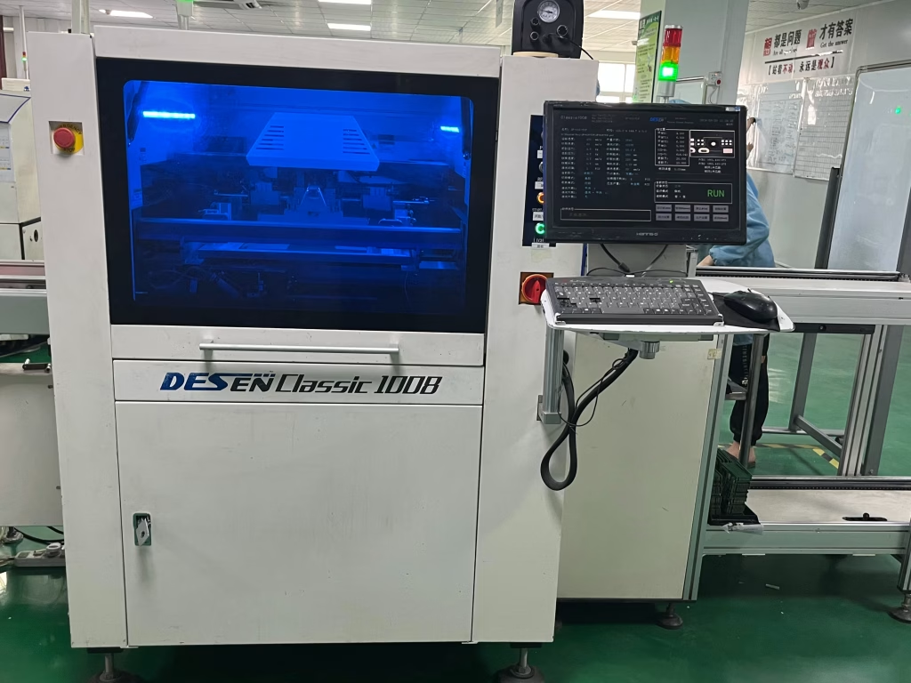
Solder Paste and Stencil Design
- Stencil thickness and apertures: Common range is 0.10–0.12 mm for fine pitch and 0402/0201. Use step stencils or aperture reductions by part type. Reduce fine‑pitch apertures 10–20% to cut bridging risk.
- Area ratio rule: Laser‑cut stencil aperture area ratio > 0.66 improves release. Nano coating can help micro‑apertures.
- Solder paste properties: Viscosity, slump, metal loading, and flux system drive print repeatability and wetting. Select proper powder type (e.g., Type 4/4.5/5) based on pitch and spacing.
Printing and SPI
- Print parameters: Fiducial alignment accuracy, squeegee pressure and speed, snap‑off, and separation speed. Use closed‑loop cleaning (e.g., auto under‑wipe every set number of boards) and re‑check fiducials.
- 3D SPI: Measure paste volume, height, area, and shape on every pad. Typical process window is ±20–30% volume, depending on component type and pad design. Close the loop to the printer to avoid passing defects downstream.
Component Placement
- Equipment capability: Mixed placement from 01005 to large BGA/QFN/connectors. Vision alignment and centering maintain positional accuracy.
- Process control: Choose the right nozzle. Tune placement force, vacuum, and Z‑height. Use soft placement and board supports for fragile parts (e.g., crystals, cameras, shields).
Reflow Soldering
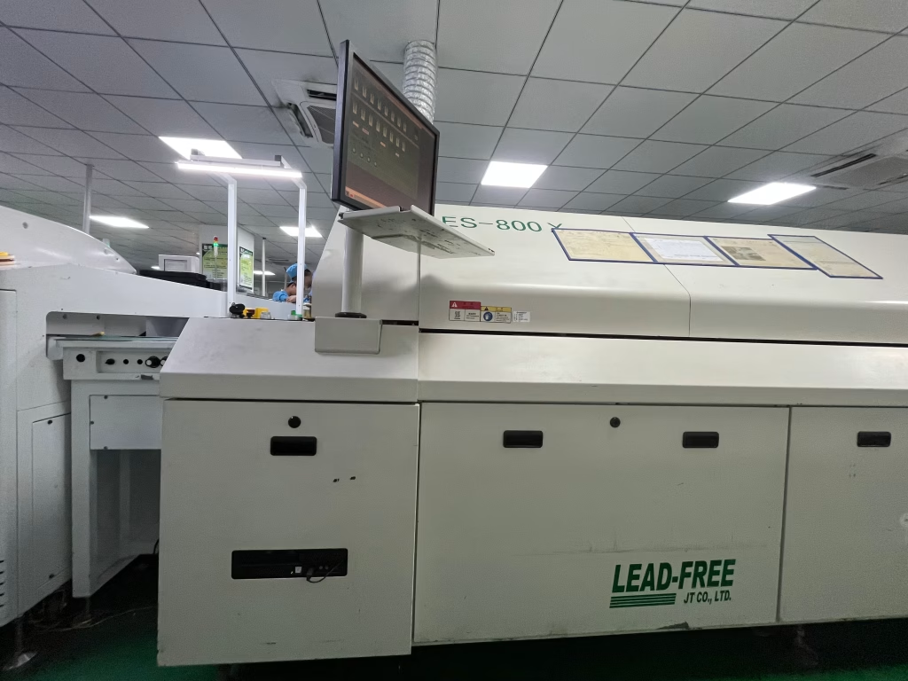
- Thermal profile: The oven ramps the board through preheat, soak, reflow, and cooling. When solder melts and wets, it forms electrical and mechanical joints.
- Profile control: Lead‑free alloys typically need higher peak temperature than leaded. Use thermocouples to profile worst‑case locations. Control delta‑T across the PCB to protect heat‑sensitive parts and laminates. Set proper time above liquidus and cool‑down rate to limit voiding and solder balls. Nitrogen atmosphere can be considered for fine‑pitch and high‑reliability needs.
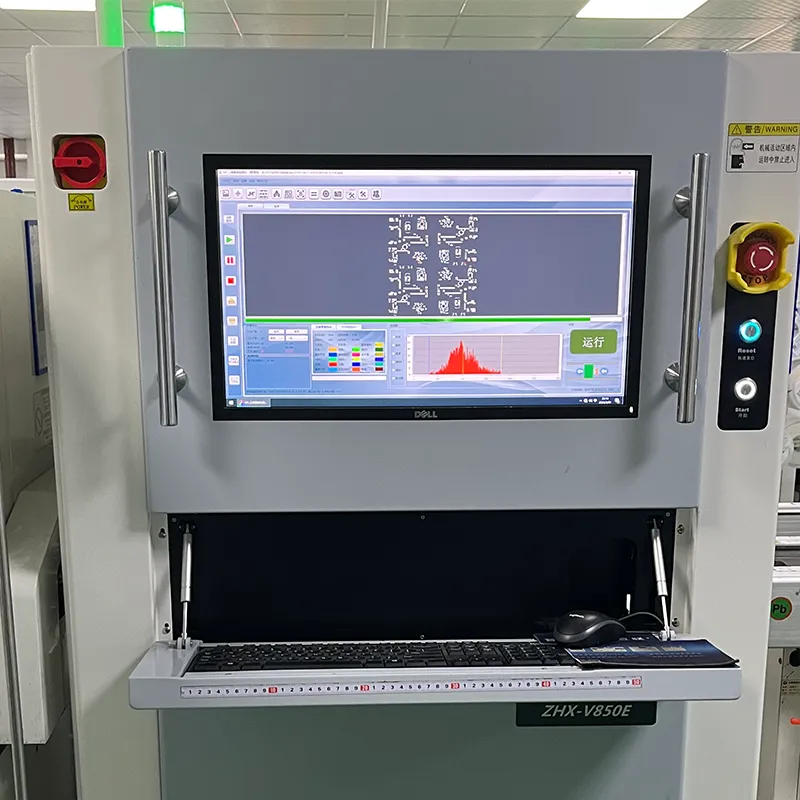
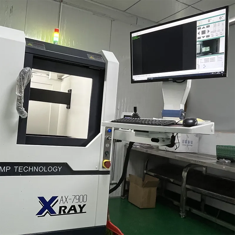
AOI and X‑Ray Inspection
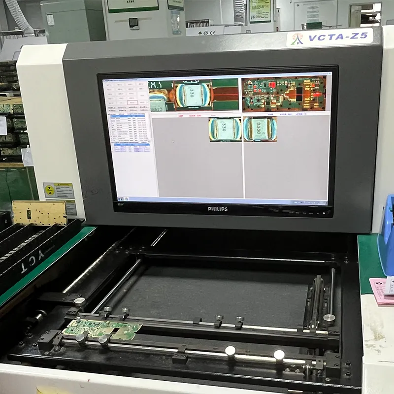
- AOI: High‑resolution cameras check presence/absence, alignment, polarity, text, and fillet shape. It catches misalignment, missing parts, tombstones, bridges, and insufficient solder.
- X‑ray: For hidden joints such as BGA and some QFN, 2D/3D X‑ray measures ball quality, voiding, opens, and shorts that optical methods cannot see.
Cleaning and Conformal Coating
- Cleaning: Use aqueous, semi‑aqueous, or solvent systems, sometimes with ultrasonics. Remove flux residues and particles to cut ionic contamination that can cause corrosion or dendritic growth. SIR/ROSE testing can validate cleanliness for high‑reliability sectors.
- Conformal coating: Choose acrylic, urethane, silicone, or parylene per environment and life requirements. Control thickness, masking, pinholes, and bubbles. Verify coverage in keep‑out zones such as connectors and test points.
Common SMT Defects: Root Causes, Detection, and Fixes
- Defect tableSolder bridging | Root causes: excess paste, misaligned stencil | Detection: AOI, SPI | Fix: adjust stencil/apertures, printing parameters
- Tombstoning | Root causes: uneven heating, unbalanced pad sizes | Detection: AOI, visual | Fix: tune reflow profile, revise land pattern
- Insufficient solder | Root causes: low paste volume, clogged stencil | Detection: SPI, AOI | Fix: clean/repair stencil, adjust print settings
- Solder balls | Root causes: fast heat/cool, paste chemistry | Detection: AOI, visual | Fix: adjust profile, review paste selection
- Misplacement | Root causes: placement accuracy, PCB warpage | Detection: AOI, visual | Fix: calibrate machine, review PCB flatness/tolerances
- Cold joints | Root causes: low peak temperature or time above liquidus | Detection: AOI, X‑ray | Fix: adjust reflow zones and conveyor speed
- Opens | Root causes: missing solder, pad contamination | Detection: AOI, X‑ray | Fix: clean pads, verify aperture design
Frequent SPI, AOI, and X‑ray keep quality stable and reduce downstream cost and field failures.
Why SMT Matters in Modern PCBA Service
- Higher component density: Small SMT packages and double‑sided assembly enable more function in smaller devices.
- Cost efficiency: Automation reduces labor and board size, saving solder and material, especially at scale.
- Better electrical performance: Shorter paths lower inductance and capacitance for higher speed and better signal integrity.
- Flexibility and innovation: SMT supports complex multilayer boards and a wide component mix. It adapts well to design changes.
- Robust reliability: With proper control, SMT forms strong joints suitable for portable and mission‑critical products. Advanced inspection reduces defect rates.
Practical DFM Checklist for SMT Projects
- Balance pad sizes for chip resistors/capacitors to prevent tombstoning.
- Define stencil aperture reductions for fine pitch and micro‑passives; consider step‑down areas.
- Lock library polarity and pin‑1 markings; add silkscreen polarity cues.
- Choose PCB finish based on paste and reliability (e.g., ENIG, OSP, ENEPIG).
- Set panelization with fiducials, tooling holes, and break‑off rails; control board warpage.
- For BGA: ensure via‑in‑pad plating and fill rules; define solder mask web and dam sizes.
- Reserve AOI sight lines; avoid tall parts blocking smaller parts.
- Add test points for ICT/FCT; define keep‑outs for coating and programming.
- Consider moisture sensitivity (MSL) handling and bake profiles.
- Specify ESD packaging and storage conditions per component sensitivity.
- Plan THT/THR for big connectors or power parts that need extra strength.
- Balance copper and thermal reliefs to minimize CTE and bow/twist.

Barry Ding
CEO
Email
WhatsApp
Facebook
Phone
Contact me
About us
We are PCBAYCT Electronics — your trusted partner in high-quality PCB & PCBA manufacturing, backed by 15+ years of expertise and industry-leading capabilities.
Contact us
to Begin your Bessiness