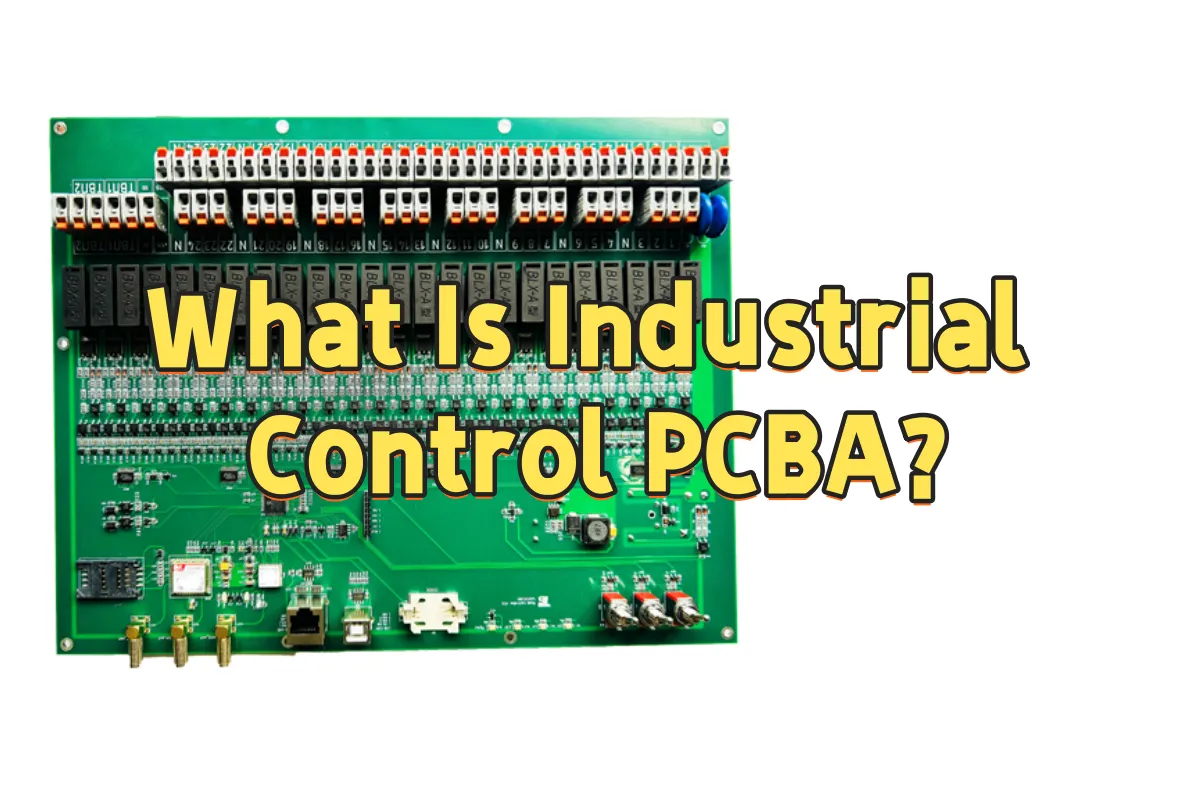
What Is an Industrial Control PCBA?
Table of Contents
What Is Industrial Control PCBA?
1. Definition & Core Functions
An Industrial Control PCBA (Printed Circuit Board Assembly) is a purpose-built electronic board that gathers data, performs logic processing, and drives motion or power inside harsh industrial environments.
Compared with consumer assemblies, an Industrial Control PCBA is engineered to survive:
| Environmental Threat | Design Counter-Measures |
|---|---|
| Mechanical shock & continuous vibration | Reinforced solder joints, anti-vibration SMT adhesives, shock-damping potting |
| Extreme temperature swings (-40 °C to +85 °C, or wider) | Wide-temperature components, metal-core or high-Tg laminates, heat-sink structures |
| High humidity & airborne dust | Conformal coating, nano-coating, or sealed enclosures to block condensation and particulates |
| Strong electromagnetic interference (EMI) | Multi-layer shielding, differential routing, controlled-impedance stacks, and solid ground isolation |
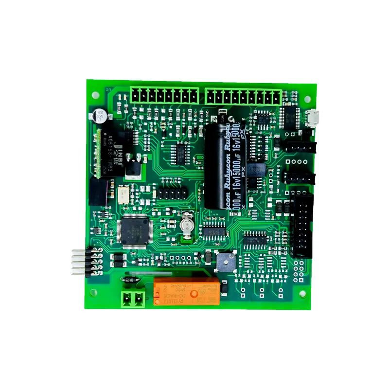
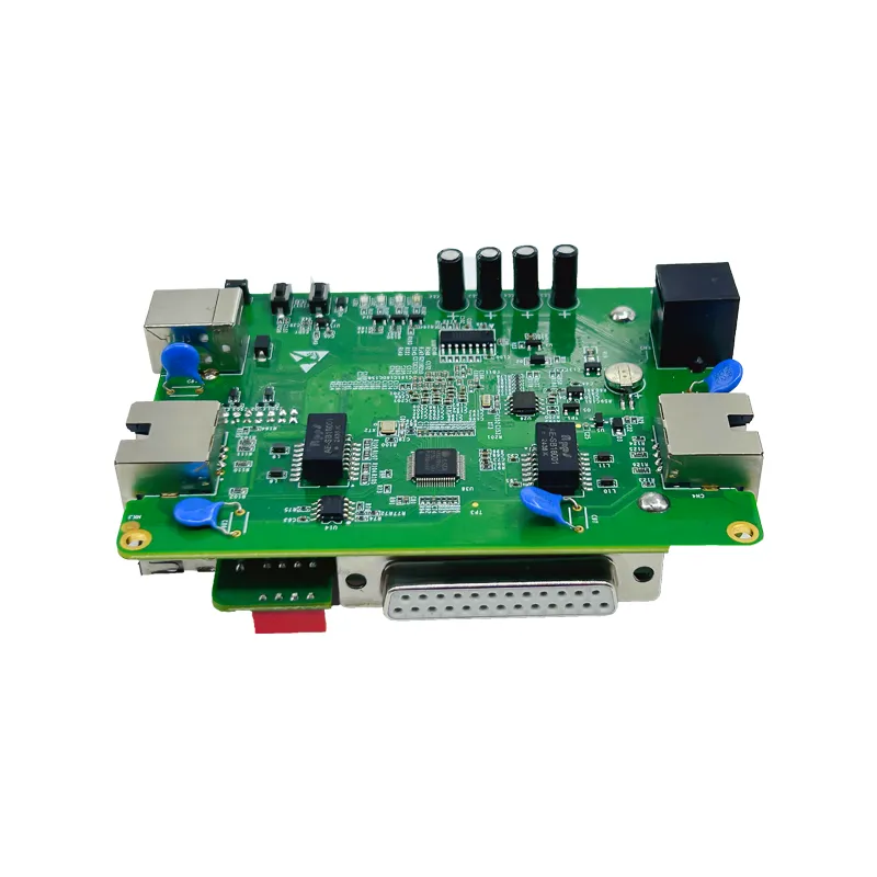
2. Structure & Materials
2.1 Layer Stack-Up
Multi-layer architecture: 4 / 6 / 8 / 10-layer stacks isolate power, ground, and high-speed traces, lowering loop impedance and boosting electromagnetic compatibility.
High-grade substrates: Mainstream FR-4 dominates, but polyimide (PI) or high-Tg hybrids (Tg ≥ 170 °C) are specified where heat or RF demands soar.
Heavy-copper areas: Standard copper starts at 1 oz ft²; power buses or relay paths often rise to 2–4 oz ft² with thermal vias for hotspot spreading.
Surface & protective finishes: ENIG, ENEPIG, or immersion tin withstand humidity and reflow heat; finished boards receive a conformal coat or nano-film for secondary protection.
2.2 Components & Assembly
Component selection: MCUs/MPUs, FPGAs, power modules, Hall sensors, and industrial-lock connectors are screened to −40 °C—+85 °C (or wider), plus salt-spray and vibration tests.
Hybrid SMT + THT: 01005 passives and high-speed ICs are placed by SMT, while large capacitors, transformers, or high-torque connectors are wave- or selective-soldered.
Mechanical reinforcement: Local epoxy dots, staking, potting, or support pillars raise shock resilience.
3. Design & Manufacturing Standards
| Standard / Regulation | Key Focus | Stage Applied |
|---|---|---|
| IPC-6012 / IPC-2221 | Base-material type, width/spacing, stack performance, solderability | PCB layout & fabrication |
| UL 94 | Flammability rating (V-0 / V-1) | Material & safety testing |
| RoHS / REACH | Limits Pb, Cd, Cr⁶⁺, PBDEs, etc., for global market access | Parts sourcing & chemistry |
| IEC 61511 (SIL) | Safety-instrumented systems integrity (SIL 1–4) | System architecture & functional-safety validation |
| IEC 61000-6-4 | Generic EMC emission limits for industrial sites | EMC design & compliance |
| EN 50155, ISO 16750 | Railway & automotive vibration/temperature/EMC | Transport & heavy-machine electronics |
4. Manufacturing & Verification Process
DFM / DFA review – impedance control, thermal modelling, test-point placement, EMC simulation.
Prototype iteration – engineering builds → small-batch pilots, each run closed with accelerated stress tests (thermal cycling, humidity bias, salt-spray, vibration).
Full-process quality loop – SPI → AOI → AXI (BGA X-ray) → ICT/FCT with MES-linked SPC charts for paste height, reflow profile, and joint integrity.
HALT / HASS – accelerated life and stress screening for MTBF prediction via Weibull modelling.
Mass-production release – PPAP / first-article approval, followed by outgoing-board audits (OBA) for every lot.
5. Key Application Domains
| Domain | Representative Equipment | Core Requirements & Value |
|---|---|---|
| Factory automation & robotics | PLCs, HMIs, 6-axis robot controllers, servo/step motor drives | Millisecond-level motion control; onboard safety interlocks avoid unplanned stops |
| Process control & instrumentation | Temperature, flow, pressure transmitters; gas analysers | Long-term drift ≤ 0.1 %; galvanic-isolated A/D; intrinsic-safe design |
| Energy & renewables | Solar inverters, storage BMS, wind-turbine pitch/yaw controllers | Thick-copper heat paths, 15-year life, IEC 62109 compliance |
| Industrial IoT | Edge gateways, multi-protocol nodes, wireless beacons | Integrated MCU/MPU + 5G / Wi-Fi 6 / LoRa; OTA updates & remote diagnostics |
| Transportation & heavy machinery | Train traction/brake PCBs, conveyor sorters, elevator masters, ECU | Shock rating up to 20 g; conformal coat vs oil mist; EN 50155 & ISO 16750 certified |
| Industrial networking | Modbus, Profibus, EtherCAT, CAN, OPC UA interface cards | Hardware time-stamp, isolated transceivers, daisy-chain or ring redundancy |
6. Assembly Workflow
PCB fabrication – lamination, imaging, CNC drilling, Cu plating, ENIG/ENEPIG, 100 % flying-probe impedance test.
Component procurement & IQC – only traceable industrial-grade parts; moisture-sensitive devices pre-baked.
SMT & THT soldering – vacuum or N₂ reflow; selective wave for large through-hole pins.
Inline inspection & functional test – AOI for solder fillets, AXI for hidden joints, ICT for shorts/opens, FCT under simulated load.
Environmental stress & reliability tests – −40↔+85 °C cycling, 85 °C/85 %RH, random vibration, drop shock; parameters must stay within ±5 %.
Conformal coating & final assembly – cured boards aged 24–72 h under full load, then packed in ESD-safe packaging.
7. Quality Assurance & Documentation
Multi-stage inspection: IQC → IPQC → OQC with AQL sampling; each board carries a unique 2-D barcode linking BOM, process parameters, and test results.
Reliability testing: 24–72 h burn-in under rated load plus HALT/HASS screens expose marginal solder joints or material fatigue early.
Transparent records: Customers may request batch reports, FMEA logs, or 8D corrective actions, all traceable for the life of the product.
8. Environmental & Regulatory Focus
RoHS / REACH compliance: third-party lab reports confirm < 0.1 % Pb, Cd, Cr⁶⁺, PBDEs.
Lead-free soldering: SAC305 or low-Ag alloys with tuned profiles maintain joint strength.
Circular materials: low-VOC inks, recyclable glass-fiber laminates, copper recovery channels; carbon-footprint audits per ISO 14064.

Barry Ding
CEO
Email
WhatsApp
Facebook
Phone
Contact me
About us
We are PCBAYCT Electronics — your trusted partner in high-quality PCB & PCBA manufacturing, backed by 15+ years of expertise and industry-leading capabilities.
Contact Us
to Begin Your Bessiness