
A Complete Guide to the PCBA Process
In the rapidly evolving world of electronics manufacturing, the Printed Circuit Board Assembly (PCBA) process stands as a cornerstone of innovation and quality. This complex yet essential procedure transforms bare circuit boards into sophisticated electronic devices that power everything from household gadgets to industrial equipment. As a leading factory specializing in PCBA assembly and production, we are committed to mastering each step of this intricate process. From meticulous circuit board design and precision component placement to rigorous quality control and environmental compliance, our focus is on delivering high-performance products that meet global market demands. This article delves into the details of the PCBA process, illustrating the journey from design to functionality and shedding light on the critical stages that define modern electronics manufacturing.
Circuit Board Design and Manufacturing
- Design Stage:
Using Electronic Design Automation (EDA) software, engineers create circuit designs and layouts, generating essential files like Gerber and drilling files to guide production. - Manufacturing Stage:
This phase involves several critical steps – printing, etching, drilling, plating, and pad coating – to ensure the board’s conductivity and stability.
Components Procurement and Inspection
- Procurement:
Components are sourced from reliable suppliers according to the Bill of Materials (BOM) list, ensuring consistent quality and compatibility. - Inspection:
Components undergo thorough inspections, including visual checks, dimensional measurements, and electrical performance tests, to ensure they meet quality standards.
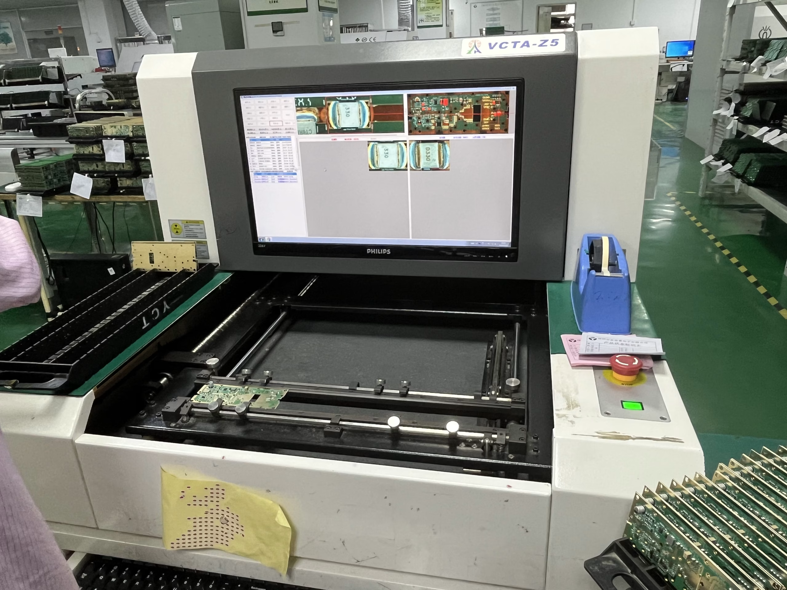
SMT Assembly Process
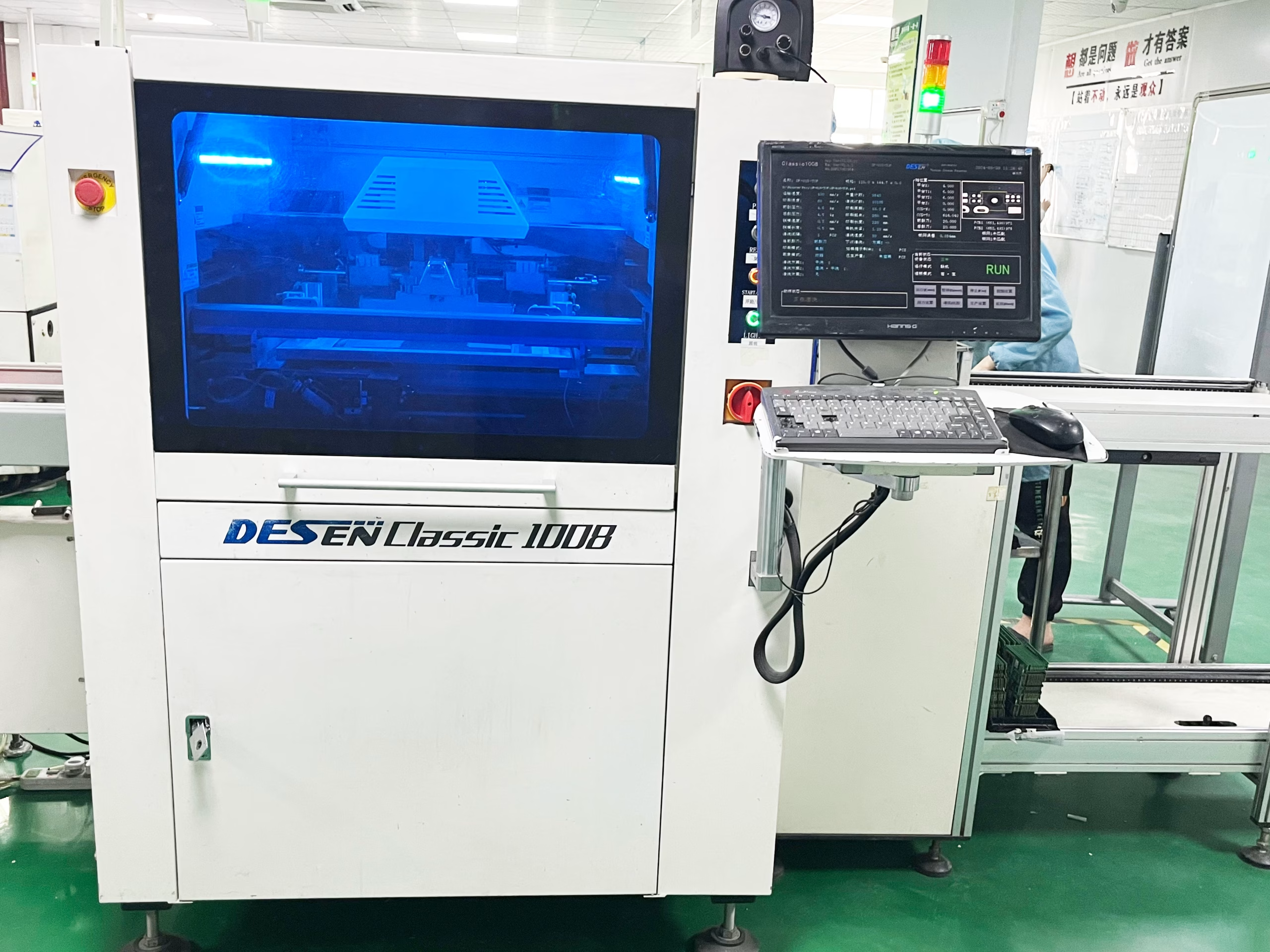
- Solder Paste Printing:
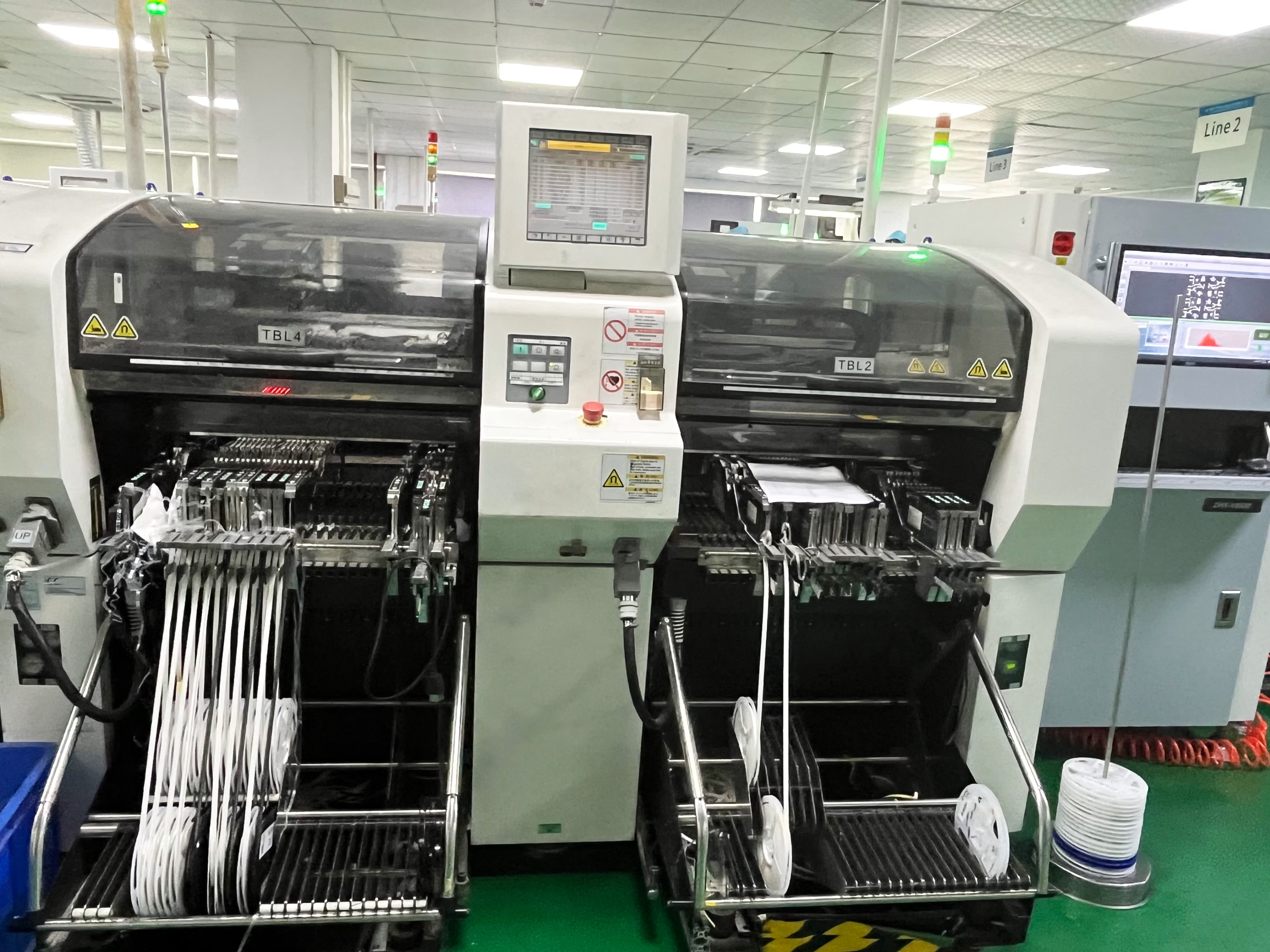
Solder paste is applied to the PCB pads to prepare for component placement. - Component Placement:
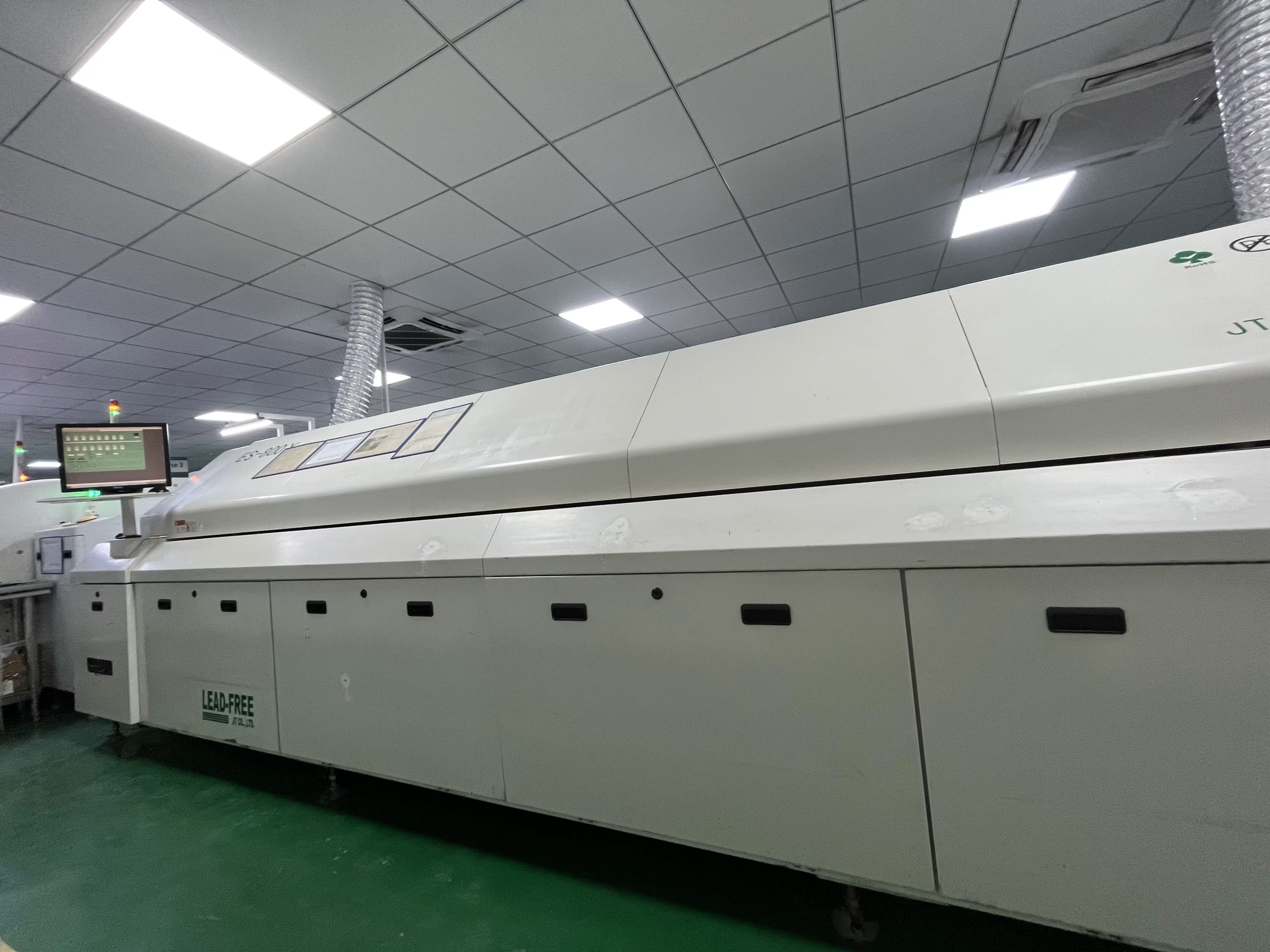
Surface Mount Technology (SMT) machines accurately place components onto the PCBs according to the design specifications. - Reflow Soldering:
The board undergoes heating to melt the solder paste, creating secure connections between components and the PCB. - Automated Optical Inspection (AOI):
This step involves checking the placement accuracy and solder quality to ensure reliability.
DIP Processing
- Insertion:
DIP components are manually or automatically inserted into PCB holes. - Wave Soldering:
Wave soldering equipment is used to solder the components onto the board securely. - Lead Trimming:
Excess leads are trimmed to improve aesthetics and connection integrity. - Post-Solder Handling:
Cleaning and inspection of the soldered areas ensure high standards are met.
Soldering Processes
- Solder Paste Application:
Solder paste is carefully applied to the PCB, preparing it for SMT processes. - Component Placement:
Assembling components on the solder paste for subsequent reflow soldering. - Reflow Soldering:
The solder paste melts upon heating, forming strong joints between components and the PCB. - Post-Solder Inspection:
The boards are cleaned, and solder joints are inspected for quality assurance.
Cleaning and Testing
- Cleaning:
Removing residues and contaminants from the soldering process ensures product integrity. - Testing:
Various tests, such as In-Circuit Testing (ICT), Functional Circuit Testing (FCT), and aging tests, confirm the PCBA’s functionality and performance.
Quality Control and Traceability
- Quality Control:
A multi-level inspection process using AOI, X-ray inspection, and in-line testing ensures product quality and reliability. - Traceability System:
Establishing a quality management system ensures every production stage is traceable, promoting accountability and continuous improvement.
Environmental and Safety Measures
- Environmental Practices:
Utilizing lead-free solder and green PCB materials, optimizing production processes to minimize energy consumption and reduce emissions. - Safety Measures:
Maintaining a safe production environment adhering to relevant regulations and standards.
The PCBA process is vital to the success of electronics manufacturing, encompassing stages from initial design to final assembly. Through detailed steps such as circuit board design, careful component procurement, and advanced SMT and DIP assembly techniques, PCBA ensures the creation of high-quality, reliable electronic products. Quality assurance and traceability are integral elements, supported by sophisticated inspection methods and a robust management system. Additionally, environmentally friendly practices and stringent safety measures are implemented to align with regulatory standards and promote sustainable manufacturing. By converting raw PCBs into functional devices, the PCBA process not only powers today’s technology but also sets the stage for future innovations in the electronics industry.